


With the rapid development of the electronics industry, SMD LED PCB (Surface Mount Device Light Emitting Diode Printed Circuit Board) has become an integral part of modern electronic devices. This article aims to provide a comprehensive introduction to the SMD LED PCB industry, covering its history, manufacturing process, applications, and future trends.
History of SMD LED PCB
The concept of surface mount technology (SMT) originated in the 1960s, and it has been evolving ever since. SMD components, including LEDs, have revolutionized the electronics industry by offering smaller, lighter, and more efficient devices. The SMD LED PCB industry has grown significantly over the past few decades, driven by the increasing demand for compact and energy-efficient electronic products.
In the early stages, SMD LED PCBs were primarily used in low-cost consumer electronics such as calculators and small toys. However, with the advancement of technology, their applications have expanded to include high-end consumer electronics, automotive, medical devices, and industrial equipment.
Manufacturing Process of SMD LED PCB
The manufacturing process of SMD LED PCBs involves several steps, each critical to the final product’s quality and performance. Here is an overview of the typical process:
1. Design: The first step is the design of the PCB layout, which includes the placement of SMD LEDs and other components on the board. CAD (Computer-Aided Design) software is commonly used for this purpose.
2. Material Selection: High-quality materials, such as copper foil, glass fiber, and soldermask, are chosen for the PCB substrate. The copper foil provides the necessary electrical connections, while the glass fiber adds structural strength.
3. Etching: The copper foil is etched to form the required circuit patterns. This process involves dipping the PCB into an etching solution and removing the unwanted copper.
4. Drilling: Holes are drilled through the PCB for component leads and vias. These holes are then plated with copper to ensure electrical connectivity.
5. Lamination: The etched and drilled PCB is laminated with prepreg material to create multiple layers of the PCB. The prepreg acts as an insulator and helps in maintaining the structural integrity of the board.
6. Soldermask Application: A soldermask is applied to the PCB to protect the copper traces and provide a surface for soldering. This layer also ensures that the solder does not flow onto unintended areas during assembly.
7. Silkscreen Printing: The PCB is then printed with silkscreen ink to provide component identification and other markings.
8. Vias and PTH (Plated Through Holes) Processing: Vias are created for through-hole connections, and PTHs are processed to ensure proper electrical connectivity.
9. Solder Paste Printing: Solder paste is applied to the PCB, which will be used for the assembly of SMD components.
10. Component Assembly: SMD LEDs and other components are mounted on the PCB using automated assembly machines.
11. Reflow Soldering: The PCB is then placed in a reflow oven to melt the solder paste and form the electrical connections between the components and the PCB.
12. Testing: The final step involves testing the PCB to ensure it meets the required specifications.
Applications of SMD LED PCB
SMD LED PCBs are widely used in various industries due to their compact size, high efficiency, and low power consumption. Some of the key applications include:
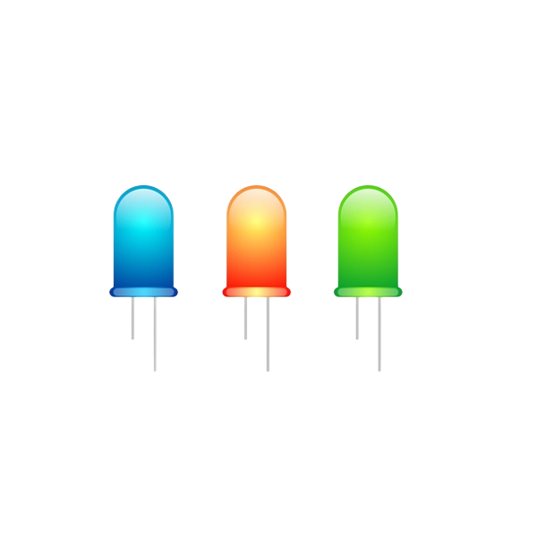
1. Consumer Electronics: Smartphones, tablets, digital cameras, and gaming consoles all utilize SMD LED PCBs for their display and lighting functions.
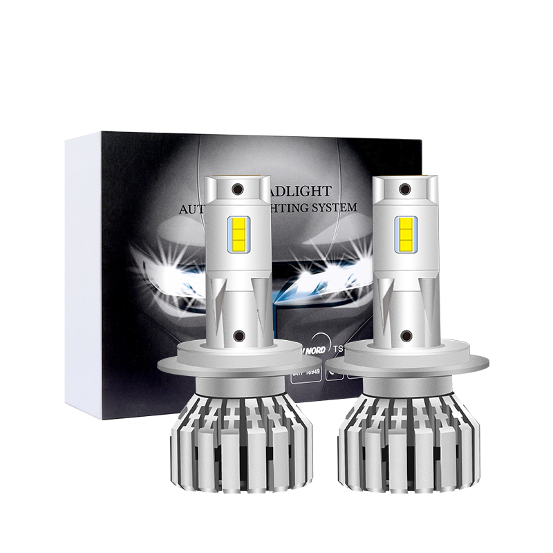
2. Automotive Industry: SMD LED PCBs are used in vehicle lighting systems, instrument clusters, and infotainment systems for their durability and energy efficiency.
3. Medical Devices: These devices often require compact and reliable PCBs for their critical functions, making SMD LED PCBs an ideal choice.
4. Industrial Equipment: Machines and control systems in industrial settings benefit from the small size and high performance of SMD LED PCBs.
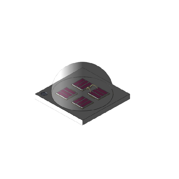
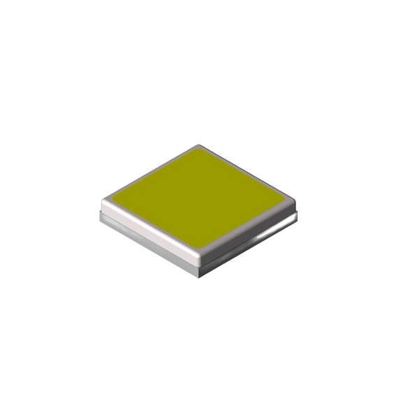
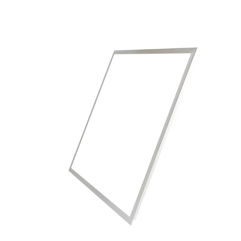
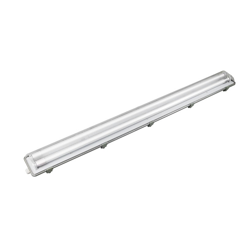
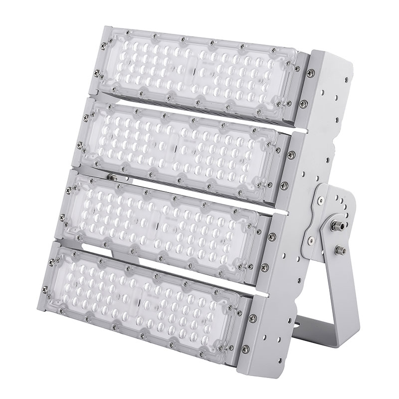
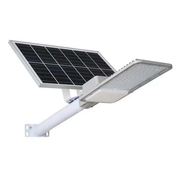
5. LED Lighting: SMD LED PCBs are used in various LED lighting products, such as streetlights, flashlights, and decorative lighting.
Future Trends in the SMD LED PCB Industry
The SMD LED PCB industry is expected to continue growing, driven by technological advancements and the increasing demand for compact and energy-efficient devices. Some of the future trends include:
1. Miniaturization: As devices become smaller, the need for miniaturized SMD LED PCBs will increase, requiring more advanced manufacturing techniques.
2. High-Density Interconnect (HDI) Technology: HDI PCBs allow for finer lines and spaces, enabling higher component density and more complex circuits.
3. Flexible PCBs: Flexible SMD LED PCBs offer greater design freedom and are ideal for applications where traditional rigid PCBs are not suitable.
4. Environmental Sustainability: As awareness of environmental issues grows, the industry is expected to focus more on sustainable materials and manufacturing processes.
5. Integration with Other Technologies: SMD LED PCBs are likely to be integrated with other technologies, such as IoT (Internet of Things) and AI (Artificial Intelligence), to create more advanced and intelligent devices.
In conclusion, the SMD LED PCB industry plays a crucial role in the electronics industry, providing the foundation for countless innovative products. With ongoing technological advancements and increasing demand, the future of SMD LED PCBs looks promising.