High power LED 660nm has become a significant topic in the lighting industry due to its unique properties and applications. This article aims to provide an in-depth introduction to the technology, its advantages, and its various applications in different fields. With a focus on the 660nm wavelength, we will explore the evolution of high power LEDs, their manufacturing process, and the future prospects of this technology.
Introduction to High Power LED 660nm
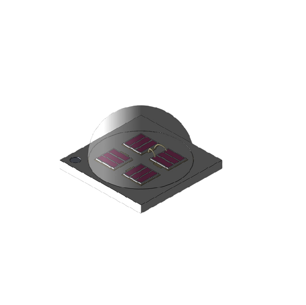
High power LED 660nm refers to an LED with a peak emission wavelength of 660 nanometers. This type of LED emits a red light with a narrow spectral bandwidth, making it ideal for various applications, including medical, horticultural, and aesthetic treatments. The high power aspect of these LEDs means they can produce a higher intensity of light compared to traditional LEDs, which allows for better performance in specific applications.
Evolution of High Power LED Technology
The evolution of high power LED technology has been a significant development in the lighting industry. Initially, LEDs were limited to low power applications due to their low luminous efficiency and limited light output. However, advancements in semiconductor materials and manufacturing processes have led to the development of high power LEDs, which can produce intense light with high efficiency.
The transition from low power to high power LEDs has been driven by the need for better performance in various applications. High power LEDs offer several advantages over traditional lighting sources, such as lower energy consumption, longer lifespan, and better color rendering. The development of high power LED 660nm has further expanded the range of applications for these devices.
Manufacturing Process of High Power LED 660nm
The manufacturing process of high power LED 660nm involves several steps, including wafer growth, epitaxial layer deposition, chip fabrication, and packaging. Here is a brief overview of each step:
1. Wafer Growth: The process begins with the growth of a single crystal semiconductor wafer using a technique called molecular beam epitaxy (MBE). This wafer serves as the base material for the LED.
2. Epitaxial Layer Deposition: The next step involves depositing a series of thin layers of semiconductor materials on the wafer using MBE. These layers are designed to create the desired optical and electrical properties of the LED.
3. Chip Fabrication: After the epitaxial layers are deposited, the wafer is diced into individual chips. This process involves cutting the wafer into small squares, each containing a single LED chip.
4. Packaging: The final step is packaging the LED chip. This involves encapsulating the chip in a protective material and connecting it to the external circuitry. The packaging process ensures that the LED can operate efficiently and reliably.
Advantages of High Power LED 660nm
High power LED 660nm offers several advantages over traditional lighting sources:
1. Energy Efficiency: High power LED 660nm consumes significantly less energy than traditional lighting sources, such as incandescent bulbs and fluorescent lamps. This makes them an environmentally friendly option for lighting applications.
2. Longevity: High power LED 660nm have a longer lifespan compared to traditional lighting sources. This reduces maintenance costs and the need for frequent replacements.
3. Color Rendering: High power LED 660nm provide excellent color rendering, which is crucial for applications such as medical and horticultural treatments. The narrow spectral bandwidth of these LEDs ensures that the emitted light is rich in red wavelengths, which are essential for specific applications.
4. Compact Size: High power LED 660nm can be designed in a compact size, making them suitable for various applications where space is limited.
Applications of High Power LED 660nm
High power LED 660nm find applications in various fields, including:
1. Medical: High power LED 660nm are used in medical applications, such as photodynamic therapy and wound healing. The red light emitted by these LEDs stimulates the production of oxygen radicals, which can help in destroying cancer cells and promoting tissue repair.
2. Horticultural: High power LED 660nm are used in horticultural applications to provide plants with the necessary light for photosynthesis. The red light emitted by these LEDs is essential for plant growth and development.
3. Aesthetic Treatments: High power LED 660nm are used in aesthetic treatments, such as skin rejuvenation and hair removal. The red light emitted by these LEDs can help in reducing wrinkles, improving skin texture, and removing unwanted hair.
4. Lighting: High power LED 660nm can be used in lighting applications, such as street lighting and architectural lighting. Their energy efficiency and long lifespan make them an ideal choice for these applications.
Future Prospects of High Power LED 660nm
The future of high power LED 660nm looks promising, with ongoing research and development aimed at improving their performance and expanding their applications. Some of the key areas of focus include:
1. Higher Efficiency: Efforts are being made to improve the luminous efficiency of high power LED 660nm, which will result in lower energy consumption and better performance.
2. Cost Reduction: As the manufacturing process becomes more efficient, the cost of high power LED 660nm is expected to decrease, making them more accessible for various applications.
3. New Applications: Ongoing research is exploring new applications for high power LED 660nm, such as in the field of optogenetics and biotechnology.
In conclusion, high power LED 660nm has emerged as a significant technology in the lighting industry, offering numerous advantages and applications. As the technology continues to evolve, we can expect to see even more innovative uses for these devices in the future.





Explore More from Queendom Lamp
Stay updated with the latest LED technology, lighting solutions, and industry insights.
Request a Quote About Queendom