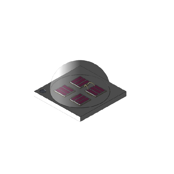
Mid-IR LED, short for mid-infrared light-emitting diode, has become a hot topic in the optoelectronics industry due to its wide range of applications. As a key component in infrared imaging and sensing systems, mid-IR LED plays a crucial role in various fields such as military, medical, industrial, and consumer electronics. This article aims to provide an in-depth introduction to the mid-IR LED industry, covering its technology, market trends, and future prospects.
Technology of Mid-IR LED
Mid-IR LED technology is based on the principle of semiconductor physics. The mid-infrared region refers to the range of electromagnetic waves with wavelengths between 2.5 and 5.0 micrometers. Compared with visible light, mid-infrared light has a longer wavelength, which allows it to penetrate through certain materials and be absorbed by others. This unique property makes mid-IR LED suitable for various applications, such as thermal imaging, gas sensing, and night vision.
Mid-IR LED devices are typically made of III-V compound semiconductors, such as InAs, InSb, and GaSb. These materials have direct bandgap structures, which enable efficient light emission in the mid-infrared region. The key to achieving high-performance mid-IR LED devices lies in the development of novel material systems, epitaxial growth techniques, and device fabrication processes.
Epitaxial Growth Techniques
Epitaxial growth is a crucial process in the fabrication of mid-IR LED devices. It involves the deposition of a thin film of semiconductor material on a substrate with a crystal lattice structure. The epitaxial layer should have a high crystal quality and good lattice matching with the substrate to ensure the electrical and optical properties of the device.
There are several epitaxial growth techniques used for mid-IR LED fabrication, including molecular beam epitaxy (MBE), metalorganic chemical vapor deposition (MOCVD), and organometallic vapor phase epitaxy (OMVPE). Each technique has its advantages and limitations. MBE is known for its high growth rate and excellent epitaxial quality, but it requires a vacuum environment and is relatively expensive. MOCVD is a widely used technique due to its lower cost and compatibility with large-scale production. OMVPE is another alternative technique that offers better material purity and less contamination.
Device Fabrication Processes
After epitaxial growth, the mid-IR LED devices need to undergo various fabrication processes to achieve the desired performance. These processes include wafer slicing, surface treatment, doping, and metalization.
Wafer slicing involves cutting the epitaxial wafer into thin slices, which will be used as substrates for the LED devices. Surface treatment is performed to improve the adhesion between the epitaxial layer and the substrate. Doping is used to create p-n junctions in the semiconductor material, which is essential for the electrical conduction. Metalization involves depositing metal contacts on the device to allow electrical current to flow.
Market Trends
The mid-IR LED market has been growing rapidly in recent years, driven by the increasing demand for infrared imaging and sensing applications. According to a report by MarketsandMarkets, the global mid-IR LED market is expected to reach USD 2.5 billion by 2025, with a CAGR of 16.3% from 2020 to 2025.
Several factors are contributing to the growth of the mid-IR LED market. Firstly, the rising demand for thermal imaging systems in military and security applications is a significant driver. Secondly, the increasing adoption of mid-IR LED-based gas sensors in industrial and environmental monitoring is also fueling market growth. Lastly, the growing popularity of consumer electronics, such as smartphones and cameras, equipped with mid-IR LED-based features is expected to further boost the market.
Future Prospects
The future of the mid-IR LED industry looks promising, with continuous technological advancements and expanding applications. Several key trends are expected to shape the industry’s development in the coming years.
Firstly, the development of high-efficiency and high-brightness mid-IR LED devices is crucial for reducing power consumption and extending battery life in portable devices. Secondly, the integration of mid-IR LED technology with other sensors and imaging systems will enable more sophisticated and intelligent applications. Lastly, the exploration of new material systems and epitaxial growth techniques will further improve the performance and cost-effectiveness of mid-IR LED devices.
In conclusion, mid-IR LED technology has a wide range of applications and holds great potential for future development. With ongoing research and innovation, the mid-IR LED industry is expected to continue its growth trajectory and contribute significantly to various fields.


