


LED 265nm has become a significant topic in the industry due to its unique properties and potential applications. This article aims to provide a comprehensive introduction to the field of LED 265nm, covering its technology, manufacturing process, and potential uses.
Introduction to LED 265nm
LEDs, or Light Emitting Diodes, are semiconductor devices that emit light when an electric current passes through them. The color of the light emitted by an LED is determined by the energy band gap of the semiconductor material used. The energy band gap is the energy difference between the valence band and the conduction band in the material. The shorter the energy band gap, the higher the energy of the emitted photons, and the shorter the wavelength of the light.
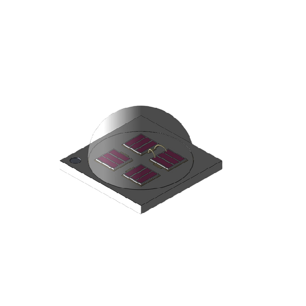
LED 265nm refers to LEDs that emit light with a wavelength of 265 nanometers. This wavelength falls within the ultraviolet (UV) spectrum, which is shorter than the visible light spectrum. LEDs with such a short wavelength are relatively rare and have limited commercial applications at present. However, their unique properties make them attractive for specific applications, such as sterilization, disinfection, and scientific research.
Technology of LED 265nm
The development of LED 265nm technology involves several challenges. Firstly, the semiconductor material with a suitable energy band gap for emitting 265nm light is difficult to find. Secondly, the material needs to be doped with impurities to achieve the desired emission properties. Finally, the manufacturing process must be optimized to ensure high efficiency and stability.
The most commonly used semiconductor material for LED 265nm is aluminum gallium indium phosphide (AlGaInP). This material has a relatively low energy band gap and can emit light with a wavelength of 265nm. To achieve the desired emission properties, the material is doped with silver or gold as a dopant. The doping process is critical to the performance of the LED, as it determines the energy band structure and the carrier concentration.
The manufacturing process of LED 265nm involves several steps, including epitaxial growth, wafer fabrication, and device assembly. Epitaxial growth is a process used to create a thin film of semiconductor material on a substrate. The wafer fabrication process involves slicing the epitaxial layer into thin wafers and preparing them for device assembly. Finally, the device assembly process involves packaging the LED chip and connecting it to the electrical circuit.
Manufacturing Process of LED 265nm
The manufacturing process of LED 265nm can be divided into the following steps:
1. Epitaxial Growth: The epitaxial growth process involves depositing a thin film of AlGaInP on a sapphire or silicon substrate. This is achieved by using a molecular beam epitaxy (MBE) or metalorganic chemical vapor deposition (MOCVD) technique. The growth parameters, such as temperature, pressure, and gas flow rate, are carefully controlled to ensure the quality of the epitaxial layer.
2. Wafer Fabrication: After epitaxial growth, the epitaxial layer is sliced into thin wafers using a diamond saw. The wafers are then polished and cleaned to remove any impurities or contaminants.
3. Device Assembly: The wafer is diced into individual LED chips using a laser cutting process. The chips are then mounted on a substrate and connected to the electrical circuit using wire bonding or flip-chip technology. Finally, the package is sealed to protect the LED chip and ensure electrical contact.
The manufacturing process of LED 265nm is highly complex and requires precise control of various parameters. The efficiency and stability of the LED are directly influenced by the quality of the epitaxial layer and the device assembly process.
Potential Applications of LED 265nm
LED 265nm has several potential applications due to its unique properties. Some of the most promising applications include:
1. Sterilization and Disinfection: LED 265nm emits light in the UV-C spectrum, which is known to be effective in destroying bacteria, viruses, and other microorganisms. This makes it suitable for use in sterilization and disinfection applications, such as water purification, air purification, and surface disinfection.
2. Scientific Research: The short wavelength of LED 265nm makes it suitable for scientific research applications, such as fluorescence microscopy, spectroscopy, and photobiology. It can be used to study the interaction between light and matter at a molecular level.
3. Industrial Applications: LED 265nm can be used in industrial applications, such as curing coatings and inks, and as a light source for photolithography. Its high energy photons can accelerate the curing process and improve the quality of the final product.
4. Environmental Protection: The use of LED 265nm in sterilization and disinfection applications can contribute to environmental protection by reducing the use of chemical disinfectants and minimizing the risk of antibiotic resistance.
Conclusion
LED 265nm is a promising technology with unique properties and potential applications. The development of LED 265nm technology involves overcoming several challenges, including the selection of suitable semiconductor materials and the optimization of the manufacturing process. As the technology continues to advance, LED 265nm is expected to find wider applications in various fields, contributing to advancements in science, industry, and environmental protection.