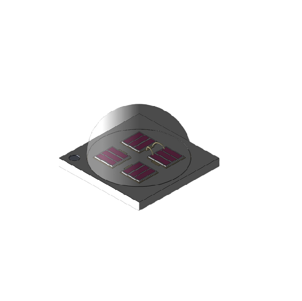
265nm LED, or ultraviolet (UV) LED, represents a cutting-edge technology in the field of lighting and optoelectronics. These LEDs emit light at a shorter wavelength, closer to the UV range, and are gaining significant attention due to their unique properties and potential applications. This article delves into the world of 265nm LED technology, exploring its characteristics, manufacturing process, and the diverse range of applications that are driving its growth in the industry.
Introduction to 265nm LED Technology
265nm LEDs are a type of UV LED that emits light at a wavelength of 265 nanometers. This wavelength falls within the UV-C range, which is known for its germicidal properties. Unlike traditional UV-C sources, such as mercury lamps, 265nm LEDs offer several advantages, including lower energy consumption, smaller size, and a longer lifespan.
Characteristics of 265nm LEDs
One of the key characteristics of 265nm LEDs is their high energy output. This is due to the short wavelength, which results in a higher photon energy. This high energy output makes them ideal for applications that require deep-penetrating UV light, such as water purification and sterilization.
Another important characteristic is their ability to produce light with a narrow spectral bandwidth. This means that 265nm LEDs emit light over a very specific range of wavelengths, which is beneficial for applications that require precise control of the UV light spectrum.
Additionally, 265nm LEDs are known for their high efficiency. They can convert a significant portion of the electrical energy they receive into light, which is a crucial factor in reducing energy costs and extending the lifespan of the devices.
Manufacturing Process of 265nm LEDs
The manufacturing process of 265nm LEDs is complex and involves several steps. It begins with the growth of a high-quality gallium nitride (GaN) substrate, which serves as the foundation for the LED structure. The GaN substrate is then patterned and etched to create the required structure for the LED.
Next, a thin layer of aluminum gallium indium nitride (AlGaN) is deposited on the GaN substrate using molecular beam epitaxy (MBE) or metalorganic chemical vapor deposition (MOCVD). This layer acts as the active region of the LED and determines the emission wavelength.
After the active region is deposited, a series of additional layers, including a cladding layer and a contact layer, are added to enhance the LED’s performance. These layers are carefully designed to optimize the LED’s efficiency, stability, and lifetime.
The final step in the manufacturing process involves encapsulating the LED with a protective material to prevent damage and enhance its environmental robustness. This encapsulation also helps to improve the LED’s thermal management and light extraction efficiency.
Applications of 265nm LEDs
265nm LEDs have a wide range of applications due to their unique properties. Some of the most prominent applications include:
- Water Purification and Sterilization: 265nm LEDs are highly effective in killing bacteria, viruses, and other pathogens in water. They are used in water purification systems, aquariums, and swimming pools to ensure clean and safe water.
- Air Purification: These LEDs can also be used to purify air by destroying harmful microorganisms, making them suitable for use in hospitals, cleanrooms, and residential spaces.
- Surface Disinfection: 265nm LEDs are used for surface disinfection in medical facilities, food processing plants, and other environments where high levels of cleanliness are required.
- UV Curing: The high energy output of 265nm LEDs makes them ideal for UV curing applications, such as printing, adhesives, and coatings. They can cure materials more quickly and efficiently than traditional UV sources.
- UV Detection and Imaging: 265nm LEDs are used in scientific research and industrial applications for detecting and imaging UV radiation, such as in astronomy and material analysis.
Challenges and Future Prospects
Despite the numerous advantages of 265nm LEDs, there are still challenges that need to be addressed. One of the main challenges is the cost of manufacturing these LEDs, which is higher compared to traditional LEDs due to the complexity of the manufacturing process. However, as the technology matures and the scale of production increases, the cost is expected to decrease.
Another challenge is the development of efficient and reliable packaging solutions for 265nm LEDs. These LEDs require specialized packaging to ensure optimal performance and longevity. Advances in packaging technology are expected to overcome this challenge.
The future of 265nm LED technology looks promising, with ongoing research and development efforts aimed at improving efficiency, reducing costs, and expanding the range of applications. As the industry continues to grow, 265nm LEDs are expected to play a crucial role in various sectors, contributing to a cleaner, safer, and more efficient world.
265nm LED technology represents a significant advancement in the field of lighting and optoelectronics. With their unique properties and potential applications, these LEDs are poised to revolutionize the way we think about UV light and its uses. As the industry continues to evolve, the future of 265nm LEDs is bright, with endless possibilities for innovation and progress.


