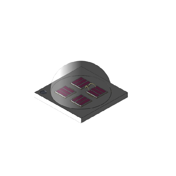
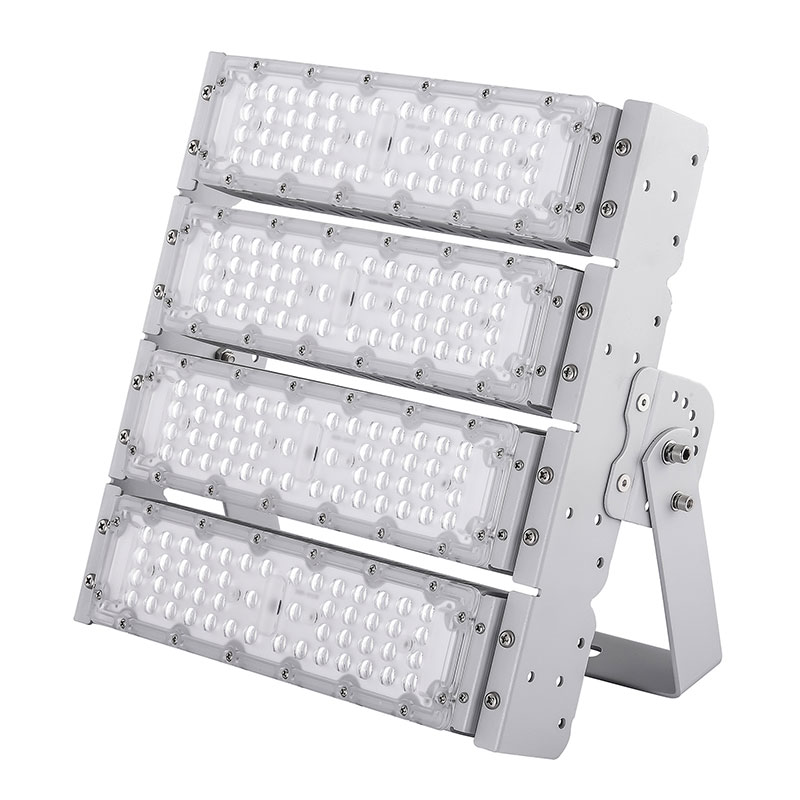
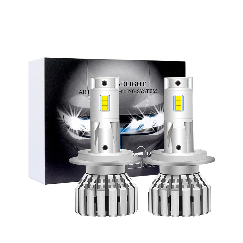
High power 405nm LED technology has emerged as a significant player in the optoelectronics industry, offering a unique combination of high brightness and precise spectral output. These LEDs, with their narrow bandwidth and intense blue light emission, have found applications in a variety of fields, including display technology, medical diagnostics, and scientific research. This article delves into the world of high power 405nm LEDs, exploring their technology, manufacturing process, applications, and the future of this rapidly evolving field.
Introduction to High Power 405nm LEDs
High power 405nm LEDs are a type of light-emitting diode that emits light at a wavelength of 405 nanometers. This wavelength falls within the blue spectral range and is particularly useful due to its ability to stimulate the phosphors in white LED packages, resulting in high-quality white light. The term “high power” refers to the ability of these LEDs to emit a significant amount of light, which is typically measured in milliwatts (mW) or watts (W).
How High Power 405nm LEDs Work
The operation of a high power 405nm LED is based on the principles of semiconductor physics. When a forward voltage is applied to the LED, electrons and holes are injected into the active region of the semiconductor material. This injection creates a recombination zone where electrons and holes recombine, releasing energy in the form of photons. In the case of a 405nm LED, the energy released corresponds to the blue light spectrum.
The key to achieving high power output lies in the design of the LED’s structure. High power 405nm LEDs often feature a multi-layer structure, which includes a p-n junction, a quantum well layer, and a cladding layer. The quantum well layer is where the recombination of electrons and holes occurs, and its thickness is optimized to produce the desired 405nm wavelength.
Manufacturing Process
The manufacturing process of high power 405nm LEDs involves several steps, including material growth, device fabrication, and packaging. Here is a brief overview of each step:
1. Material Growth: The first step is the growth of the semiconductor material, typically gallium nitride (GaN), which is the active layer of the LED. This is typically done using a chemical vapor deposition (CVD) process.
2. Device Fabrication: Once the material is grown, it is patterned and etched to create the necessary electrical contacts and optical cavity. This process often involves photolithography, etching, and doping techniques.
3. Packaging: The final step is packaging, which involves mounting the LED die onto a substrate, attaching electrical leads, and encapsulating the device in a protective material. This ensures the LED’s longevity and protects it from environmental factors.
Applications of High Power 405nm LEDs
High power 405nm LEDs have a wide range of applications due to their unique properties. Some of the most notable applications include:
1. Display Technology: In LCD displays, 405nm LEDs are used to excite blue phosphors, which in turn emit white light. This is particularly important in high-resolution displays, such as those used in smartphones and televisions.
2. Medical Diagnostics: The precise spectral output of 405nm LEDs makes them ideal for medical applications, such as fluorescence microscopy and optical coherence tomography (OCT).
3. Scientific Research: In scientific research, 405nm LEDs are used in a variety of experiments, including photochemical reactions and biological studies.
4. Agriculture: These LEDs can be used to create artificial light sources for plant growth, providing a controlled and efficient way to cultivate plants in indoor environments.
Challenges and Future Prospects
Despite their many advantages, high power 405nm LEDs face several challenges. One of the primary challenges is the thermal management of these devices. As they emit a significant amount of light, they also generate a considerable amount of heat, which can degrade the LED’s performance and lifespan.
Another challenge is the cost of manufacturing. High power 405nm LEDs require advanced manufacturing processes and high-quality materials, which can drive up the cost of production.
Looking to the future, the industry is working on several technologies to address these challenges. Advances in material science and manufacturing processes are expected to improve the efficiency and lifespan of high power 405nm LEDs. Additionally, the development of new cooling techniques and more efficient packaging solutions will help mitigate thermal issues.
In conclusion, high power 405nm LEDs are a critical component in the optoelectronics industry, offering a unique combination of high brightness and precise spectral output. As technology continues to advance, these LEDs are expected to find even more applications, driving innovation in a variety of fields.


