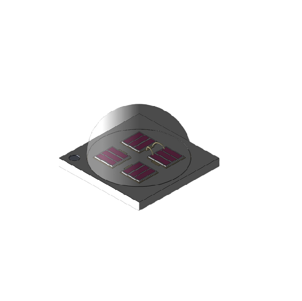
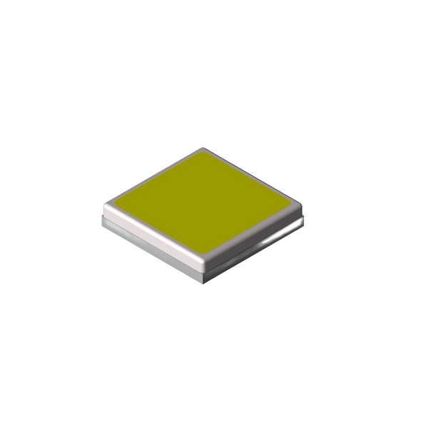
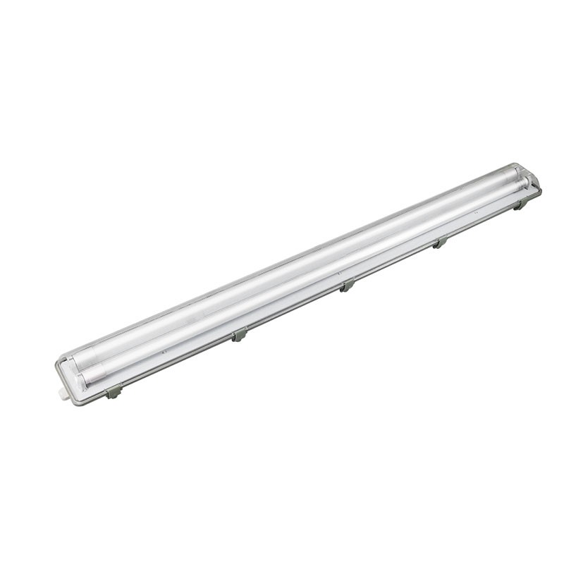
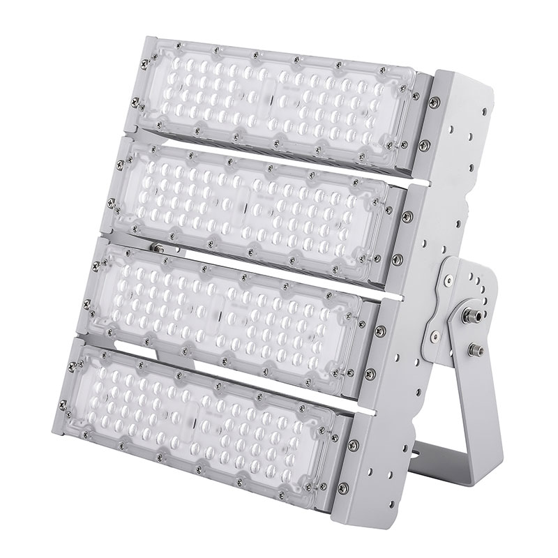
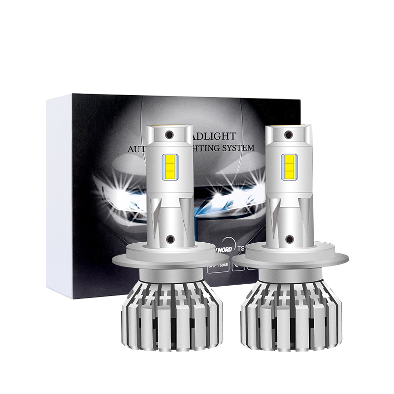
SMD LED PCB, or Surface Mount Device Light Emitting Diode Printed Circuit Board, has become an integral part of the modern electronics industry. This innovative technology has revolutionized the way light-emitting diodes (LEDs) are mounted and integrated into various electronic devices. This article delves into the details of SMD LED PCBs, their applications, manufacturing processes, and the future trends in this rapidly evolving field.
Introduction to SMD LED PCB
SMD LED PCBs are designed to efficiently mount and connect LED devices to a printed circuit board (PCB). Unlike traditional through-hole technology, SMD technology allows for smaller, more compact devices with improved performance and reliability. SMD LEDs are widely used in various applications, including automotive, medical, consumer electronics, and industrial sectors.
Applications of SMD LED PCB
The versatility of SMD LED PCBs makes them suitable for a wide range of applications. Here are some of the most common uses:
-
Automotive Industry: SMD LED PCBs are used in automotive lighting systems, including headlights, taillights, and indicator lights. They offer better illumination, lower power consumption, and longer lifespan compared to traditional bulbs.
-
Medical Equipment: In the medical field, SMD LED PCBs are used in imaging devices, surgical lighting, and patient monitoring systems. Their compact size and energy efficiency make them ideal for these applications.
-
Consumer Electronics: SMD LED PCBs are found in TVs, computers, smartphones, and other consumer electronics, where they are used for display and indicator lighting.
-
Industrial Applications: SMD LED PCBs are used in industrial equipment for lighting, control panels, and signal indicators. They offer robust performance in harsh environments.
Manufacturing Process of SMD LED PCB
The manufacturing process of SMD LED PCBs involves several steps to ensure high-quality and reliable products. Here is an overview of the process:
-
Design and Layout: The first step is to design the PCB layout using specialized software. This includes placing the SMD LED components and routing the connections.
-
Photo Imaging: The PCB design is then transferred onto a substrate using a photolithography process. This creates a pattern that will guide the etching and copper plating processes.
-
Etching and Copper Plating: The substrate is etched to remove unwanted copper, and copper is then plated onto the exposed areas to form the traces and pads.
-
Solder Mask Application: A solder mask is applied to protect the copper traces and pads from solder during assembly.
-
Drilling and Vias: Holes are drilled for vias, which allow electrical connections between different layers of the PCB.
-
Surface Treatment: The PCB surface is treated to improve solderability and prevent oxidation.
-
Component Mounting: The SMD LED components are mounted onto the PCB using automated machines.
-
Soldering: The components are soldered in place using reflow soldering or wave soldering techniques.
-
Testing and Quality Control: The PCBs are tested for functionality and quality before they are shipped to customers.
Advantages of SMD LED PCB
SMD LED PCBs offer several advantages over traditional PCB technologies:
-
Miniaturization: SMD technology allows for smaller and more compact devices, which is crucial in today’s space-constrained electronics.
-
Higher Density: SMD components can be placed much closer together, allowing for higher circuit density and more complex designs.
-
Improved Performance: SMD LED PCBs offer better thermal management, reduced electromagnetic interference, and higher reliability.
-
Cost-Effective: The smaller size and higher density of SMD components can lead to lower manufacturing costs.
Challenges and Future Trends
Despite the many advantages, the SMD LED PCB industry faces several challenges. These include the need for advanced manufacturing techniques, environmental concerns related to the use of lead-based solders, and the increasing demand for energy-efficient and durable products.
Some of the future trends in the SMD LED PCB industry include:
-
Advanced Materials: The development of new materials for PCB substrates, such as high-frequency laminates and high-temperature materials, will enable the creation of more advanced and reliable SMD LED PCBs.
-
Environmental Compliance: As environmental regulations become stricter, the industry will need to adopt more eco-friendly manufacturing processes and materials.
-
Smart Manufacturing: The integration of automation, robotics, and artificial intelligence in the manufacturing process will improve efficiency and reduce costs.
-
Customization: As the market becomes more segmented, there will be a growing demand for customized SMD LED PCB solutions to meet specific application requirements.
In conclusion, SMD LED PCBs have become a cornerstone of the modern electronics industry, offering numerous benefits that have driven innovation and efficiency. As technology continues to evolve, the SMD LED PCB industry will undoubtedly face new challenges and opportunities, shaping the future of electronics manufacturing.


